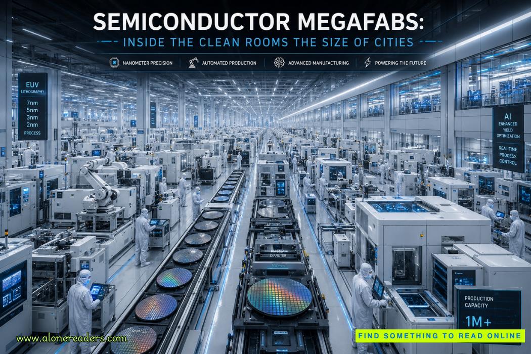
Semiconductor megafabs represent one of the most complex and capital-intensive engineering achievements in human history. These facilities are not just factories; they are vast, self-contained ecosystems designed to manufacture integrated circuits at scales measured in nanometers. When people describe them as “clean rooms the size of cities,” the phrase is not an exaggeration. Some advanced fabrication plants span hundreds of thousands of square meters, with cleanroom spaces alone rivaling the footprint of large urban districts.
At the heart of a megafab lies the cleanroom, a highly controlled environment where airborne particles are meticulously minimized. The reason is simple but unforgiving: a single dust particle can destroy an entire microchip. Modern semiconductor features are so small that even microscopic contaminants can cause fatal defects. To put it into perspective, the air inside a high-grade cleanroom is thousands of times cleaner than that of a hospital operating theater.
The classification of cleanrooms is based on the number of particles per cubic meter. Advanced semiconductor facilities often operate at ISO Class 1 or Class 2 levels, where only a handful of particles larger than 0.1 microns are allowed. Maintaining such purity requires a combination of high-efficiency particulate air (HEPA) and ultra-low penetration air (ULPA) filtration systems. These systems constantly circulate and cleanse the air, often replacing the entire volume multiple times per minute.
However, cleanliness is not just about air filtration. The entire architecture of a megafab is engineered to control contamination. Floors, walls, and ceilings are made from specialized materials that do not shed particles. Workers wear full-body suits, including gloves, masks, and boots, collectively known as “bunny suits,” to prevent human contamination. Even then, human presence is minimized as much as possible, with automation taking over many tasks.
Automation is a defining feature of semiconductor megafabs. Unlike traditional manufacturing plants, where human labor plays a central role, megafabs rely heavily on robotics and autonomous systems. Overhead transport systems move silicon wafers between processing stations in sealed pods. These systems operate continuously, orchestrated by sophisticated software that ensures optimal workflow and minimal delays.
The production process itself is staggeringly complex, involving hundreds or even thousands of steps. Each wafer undergoes repeated cycles of photolithography, etching, doping, deposition, and polishing. Photolithography, in particular, is the most critical and technologically advanced step. It involves projecting patterns onto silicon wafers using extreme ultraviolet (EUV) light. The machines used for this process are among the most expensive ever built, costing hundreds of millions of dollars each.
Temperature and humidity control are also crucial. Even slight variations can affect the precision of the manufacturing process. Megafabs maintain extremely stable environmental conditions, often within fractions of a degree Celsius and minimal humidity fluctuations. This level of control ensures that materials behave predictably and that nanoscale features are accurately reproduced.
Water and chemical management is another critical aspect. Semiconductor manufacturing consumes vast quantities of ultra-pure water, which is used to rinse wafers at various stages. This water must be purified to an extraordinary degree, removing even the smallest traces of contaminants. Similarly, the chemicals used in the process must meet stringent purity standards, as impurities can compromise the integrity of the chips.
Energy consumption in megafabs is enormous. These facilities operate 24/7 and require a continuous supply of electricity to power equipment, maintain cleanroom conditions, and support cooling systems. A single megafab can consume as much energy as a small city. As a result, energy efficiency and sustainability have become increasingly important considerations. Many companies are investing in renewable energy sources and advanced energy management systems to reduce their environmental impact.
The scale of these facilities extends beyond physical size. The investment required to build a cutting-edge megafab can exceed $20 billion. This includes not only the construction of the facility but also the acquisition of specialized equipment and the development of supporting infrastructure. Governments often play a role in supporting these projects, recognizing their strategic importance in the global economy.
Supply chain integration is another defining characteristic of megafabs. These facilities depend on a vast network of suppliers for raw materials, chemicals, equipment, and services. Any disruption in this network can have significant consequences, as seen during global semiconductor shortages. To mitigate risks, companies are increasingly focusing on supply chain resilience, including diversification and localization strategies.
One of the most fascinating aspects of megafabs is their resemblance to miniature cities. They have their own internal logistics systems, waste management processes, and even dedicated teams for infrastructure maintenance. Some facilities include amenities such as cafeterias, medical centers, and training facilities for employees. This self-contained nature allows them to operate with high efficiency and minimal external dependencies.
The workforce within a megafab is highly specialized. Engineers, technicians, and scientists work together to ensure the smooth operation of the facility. Their roles range from equipment maintenance and process optimization to quality control and research and development. Continuous training is essential, as the technology evolves rapidly and requires constant adaptation.
Despite their sophistication, megafabs face several challenges. One of the most significant is the increasing complexity of semiconductor design and manufacturing. As chip features shrink further, the margin for error becomes even smaller. This requires ongoing innovation in materials, processes, and equipment.
Another challenge is geopolitical. Semiconductor manufacturing has become a critical component of national security and economic competitiveness. Countries are investing heavily in domestic production capabilities to reduce reliance on foreign suppliers. This has led to a wave of new megafab projects around the world, each aiming to secure a share of the global semiconductor market.
Environmental concerns also play a growing role. The resource-intensive nature of semiconductor manufacturing raises questions about sustainability. Companies are exploring ways to reduce water usage, recycle materials, and minimize emissions. Innovations in green manufacturing practices are becoming a key focus area.
Looking ahead, the evolution of megafabs will likely be shaped by emerging technologies such as artificial intelligence and advanced automation. These technologies can enhance process control, improve efficiency, and reduce defects. Additionally, new materials and manufacturing techniques may redefine the limits of what is possible in semiconductor production.
An example that illustrates the scale and complexity of a megafab is a leading-edge facility producing 3-nanometer chips. Such a facility may house thousands of tools, process tens of thousands of wafers per month, and operate with near-perfect precision. Each wafer can contain hundreds of individual chips, each with billions of transistors. The coordination required to achieve this level of output is nothing short of extraordinary.
Semiconductor megafabs are more than just manufacturing plants; they are the backbone of the modern digital world. From smartphones and laptops to cars and medical devices, nearly every aspect of contemporary life depends on the chips produced in these facilities. As demand for advanced electronics continues to grow, the importance of megafabs will only increase.
Understanding these facilities offers a glimpse into the future of technology and industry. They embody the convergence of engineering, science, and innovation on a scale that few other industries can match. In many ways, they are the hidden cities powering the digital age, operating silently yet indispensably behind the scenes.

January 02, 2025

October 25, 2023


 Doggerland Lost World: The Sunken Heart of Ice Age Europe
 Sundaland Sunken World: Ancient Seafarers Before History
 New Deep Sea Species Found in the Clarion-Clipperton Zone
 LiDAR Lost City Discoveries Explained
 Fastnet Lighthouse: Ireland’s Lighthouse of the Open Atlantic and Guardian of the Western Seas
 Heceta Head Lighthouse: Oregon’s Scenic Coastal Landmark and Maritime Beacon
 Harold Godwinson: The Last Anglo-Saxon King of England
 The Three Claimants to the English Throne: Harold Godwinson, William of Normandy, and Harald Hardrada
 England Before Hastings: Edward the Confessor’s Death and the Succession Crisis
 The Battle of Hastings (1066): The Battle That Changed England Forever
 The Role of Indian Princes, Sikhs, and Gurkhas During the Indian Rebellion of 1857
 Regional Uprisings Across India: Central India, Rohilkhand, and the Expanding Revolt of 1857
 Kunwar Singh and the Rebellion in Bihar: The Elder Warrior Who Challenged British Rule
 The Battle of Gwalior and the Final Stand of the Rebel Leaders (1858)
 The Sassanid Empire: Persia’s Fire Worshipers and the Arab Conquests
 The Rise and Fall of the Holy Roman Empire: A Fragmented Power